Design an Amplifier and second-order Butterworth filter using cadence
- nsnkoduru
- Jan 25, 2025
- 2 min read
Abstract
In this project, we simulate a 2-stage miller compensated amplifier with cadence to
familiar with the program, investigate the behavior of the structure, and calculate
essential parameters of the designed opamp. Then we imply the opamp to model a
second order Butterworth filter.
Introduction
At first, I start to set the cadence and create the directory, test bench, and library
that we need Based on the script. Then I follow the instructions to sketch the
circuit and the biasing. After this step and passing the debugging process A dc,
noise, and AC analysis is done.
Design protocol:
Based on class notes and tutorial I follow these equations to reach the
requirements:
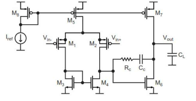

Fig1 shows the test bench of the cadence.


Figure 2:miller capacitor adjustment
For setup the miller capacitor with mim model the width of capacitor set to
15.59um and length of 25.105um to reach 380.037fF capacitor.


ALL transistors are in saturation and dc operating points are illustrated.


The PM of first design is below the requirement which is 45 degree therefore by increase the output stage gm and the PM of 57.858 degree at 573.95MHz achieved.


Conclusion
Based on simulation results this amplifier works on saturation region and input-referred noise is in the acceptable range of 1.07. The dc gain is 75dB and PM =57.585° noise at f=864.345hz reach to minimum.
the minimum requirements and simulated parameters are listed below:


Comments